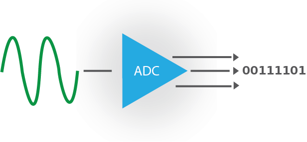
Раскладываем по полочкам параметры АЦП
Время на прочтение
10 мин
Количество просмотров 60K
Привет, Хабр! Многие разработчики систем довольно часто сталкиваются с обработкой аналоговых сигналов. Не все манипуляции с сигналами можно осуществить в аналоговой форме, поэтому требуется переводить аналог в цифровой мир для дальнейшей постобработки. Возникает вопрос: на какие параметры стоит обратить внимание при выборе микроконтроллера или дискретного АЦП? Что все эти параметры означают? В этой статье постараемся детально рассмотреть основные характеристики АЦП и разобраться на что стоит обратить внимание при выборе преобразователя.
Введение
Начать бы хотелось с интересного философского вопроса: если аналоговый сигнал — это бесконечность, теряем ли мы при оцифровке сигнала бесконечное количество информации? Если это так, тогда какой смысл существования такого неэффективного преобразования?
Для того, чтобы ответить на этот вопрос, разберемся с тем, что такое аналого-цифровое преобразование сигнала. Основной график, который отражает работу АЦП – передаточная характеристика преобразования. В идеальном мире это была бы прямая линия, то есть у каждого аналогового уровня сигнала имелся бы единственный цифровой эквивалент.

Рис. 1: Идеальная характеристика АЦП
Однако из-за наличия различных видов шума, мы не можем увеличивать разрядность АЦП до бесконечности. То есть существует предел, который ограничивает минимальную цену деления шкалы. Другими словами, уменьшая деление шкалы мы рано или поздно «упремся» в шум. Да, конечно, можно сделать хоть 100-битный АЦП, однако большинство бит данного АЦП не будут нести полезную информацию. Именно поэтому характеристика АЦП имеет ступенчатую форму, что равносильно наличию конечной разрядности АЦП.
Проектируя систему необходимо выбирать АЦП, который бы обеспечил отсутствие потери информации при оцифровке. Для того, чтобы выбрать преобразователь, необходимо понять, какие параметры его характеризуют.
Параметры АЦП можно разделить на 2 группы:
- Статические — характеризуют АЦП при постоянном или очень медленно изменяющемся входном сигнале. К данным параметрам можно отнести: максимальное и минимальное допустимое значение входного сигнала, разрядность, интегральную и дифференциальную нелинейности, температурную нестабильность параметров преобразования и др.
- Динамические — определяют максимальную скорость преобразования, предельную частоту входного сигнала, шумы и нелинейности.
Статические параметры
- Максимальный (Vref) и минимальный (обычно 0) уровни входного сигнала — устанавливают диапазон шкалы преобразования, относительно которой будет оцениваться входной сигнал (рис. 1). Также этот параметр может обозначаться как FS — full scale. Для дифференциального АЦП шкала определяется от -Vref до +Vref, однако для упрощения далее будем рассматривать только single-ended шкалы.
- Разрядность (N) — разрядность выходного кода, характеризующая количество дискретных значений (
 ), которые преобразователь может выдать на выходе (рис. 1).
 - Ток потребления (Idd) — сильно зависит от частоты преобразования, поэтому информацию об этом параметре лучше искать на соответствующем графике.
- МЗР (LSB) – младший значащий разряд (Least Significant Bit) — минимальное входное напряжение, разрешаемое АЦП (по сути единичный шаг в шкале преобразования). Определяется формулой: (рис. 1).
- Ошибка смещения (offset error) – определяется как отклонение фактической передаточной характеристики АЦП от передаточной характеристики идеального АЦП в начальной точке шкалы. Измеряется в долях LSB. При ошибке смещения переход выходного кода от 0 в 1 происходит при входном напряжении отличном от 0.5LSB (рис. 2).
 Рис. 2: Ошибка смещения
Существует и другой вариант квантователя, когда переход осуществляется при целых значения LSB (характеристика у него будет смещена относительно первого варианта, который представлен на рисунке 2). Оба этих квантователя равноправны, и для простоты далее будем рассматривать только первый вариант. - Ошибка усиления (gain error) – определяется как отклонение средней точки последнего шага преобразования (которому соответствует входное напряжение Vref) реального АЦП от средней точки последнего шага преобразования идеального АЦП после компенсации ошибки смещения (рис. 3).
Рис. 3: Ошибка усиления
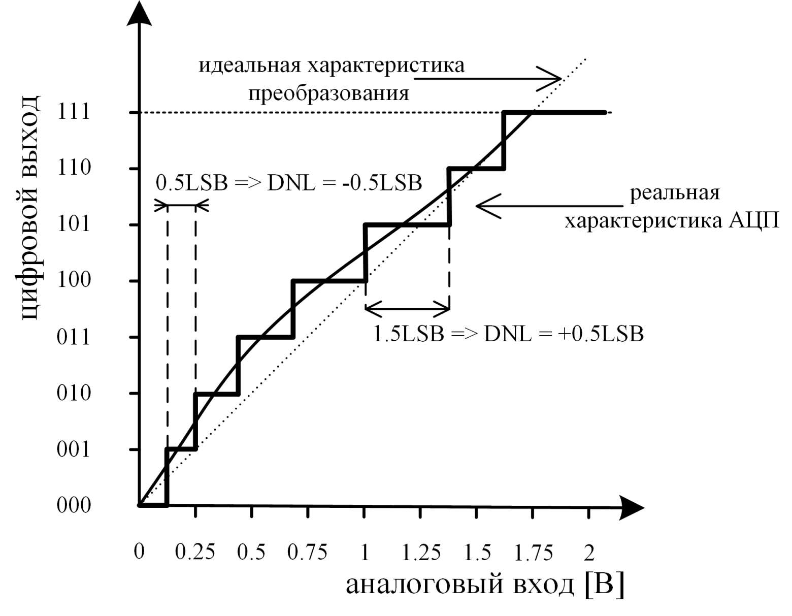
- Дифференциальная нелинейность (DNL — Differential nonlinearity) – отклонение ширины ступеньки на передаточной характеристике реального АЦП от номинальной ширины ступеньки у идеального преобразователя. Из-за дифференциальной нелинейности шаги квантования имеют различную ширину (рис. 4).

Рис. 4: Дифференциальная нелинейность
Для 3-х битного АЦП с рисунка 4:
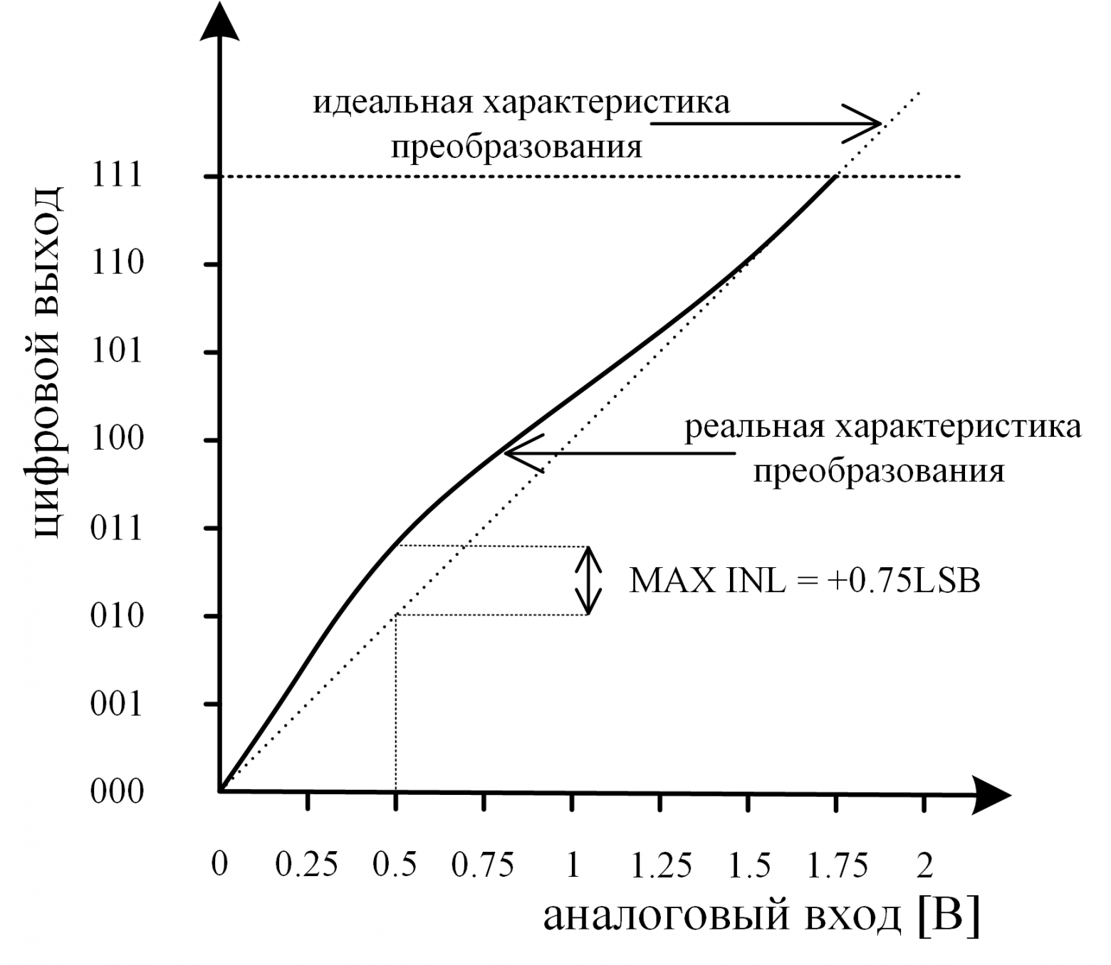
- Интегральная нелинейность ( INL — Integral nonlinearity) – разница по вертикали между реальной и идеальной характеристикой преобразования (рис. 5). INL можно интерпретировать как сумму DNL. Отрицательная INL указывает на то, что реальная характеристика находится ниже идеальной в данной точке шкалы. Для положительной INL реальная характеристика находится выше идеальной. Распределение DNL определяет интегральную нелинейность АЦП.
Рис. 5: Интегральная нелинейность
- Общая нескорректированная ошибка ( TUE — Total Unadjusted Error) – абсолютная ошибка, включающая в себя следующие ошибки: квантования, смещения, усиления и нелинейности. Другими словами, это максимальное отклонение между реальной и идеальной характеристикой преобразования. Для идеального АЦП TUE = 0.5LSB, обусловлена ошибкой квантования (или шум квантования — возникает из-за округления значения аналогового сигнала, которое соответствует цифровому коду). Ошибки усиления и смещения обычно вносят наиболее весомый вклад в абсолютную ошибку. Однако с точки зрения динамических параметров (см. ниже) ошибки смещения и усиления ничтожны, так как они не порождают нелинейных искажений.
 ), которые преобразователь может выдать на выходе (рис. 1).
 (рис. 1).
 Рис. 2: Ошибка смещения
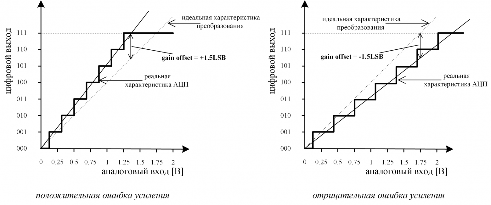 Рис. 3: Ошибка усиления

Динамические параметры
- Частота дискретизации (fs — sampling frequency) — частота, при которой происходит преобразование в АЦП (ну или 1/Ts, где Ts — период выборки). Измеряется числом выборок в секунду. Обычно под данным обозначением подразумевают максимальную частоту дискретизации, при которой специфицированы параметры преобразователя (рис. 6).

Рис. 6: Процесс преобразования АЦП
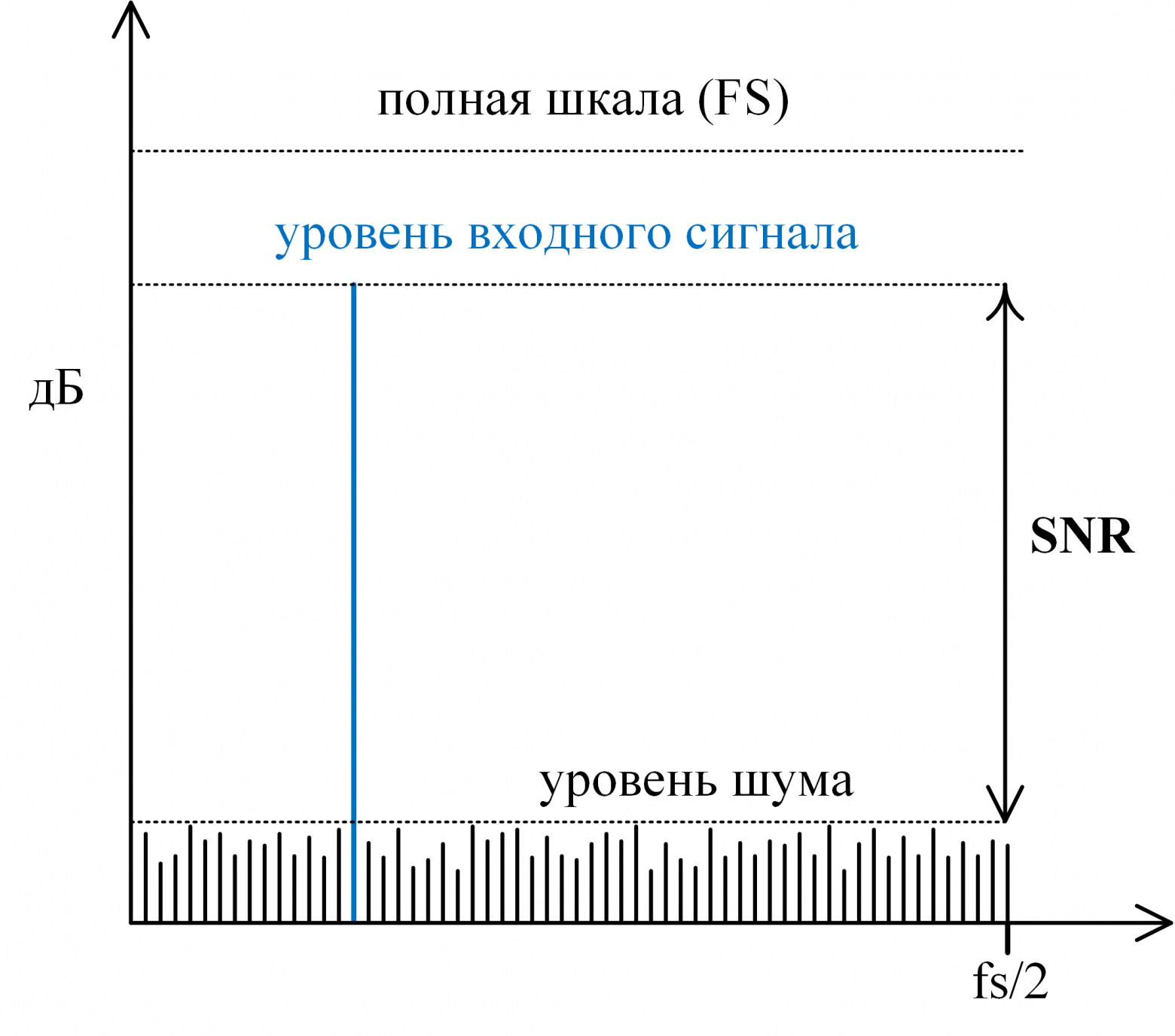
- Отношение сигнал/шум (SNR — Signal-to-Noise Ratio) — определяется как отношение мощности обрабатываемого сигнала к мощности шума, добавляемого в процессе преобразования. SNR обычно выражается в децибелах (дБ) и рассчитывается по следующей формуле:
Наглядно данное выражение продемонстрированно на рисунке 7.

Рис. 7: Отношение сигнал/шум
Для оценки SNR АЦП при разработке системы можно воспользоваться следующей формулой:
Первые 2 слагаемых учитывают уровень сигнала и ошибку квантования (нужно понимать, что формула верна для сигнала размаха полной шкалы). Третье слагаемое учитывает эффект передискретизации (выигрыш по обработке или processing gain): если полоса обрабатываемого сигнала (BW < fs/2), то, применив цифровой фильтр низких частот (либо полосовой, тут зависит все от полосы и несущей) к результату преобразования, можно вырезать часть шума АЦП, а оставшаяся часть будет распределена от 0 до BW (рис. 8). Если шум АЦП равномерно распределен по всем частотам (т.н. «белый» шум) интегральный шум после фильтрации уменьшится в fs/2 / BW раз, что и отражает третий член формулы.
Рис. 8: Увеличение SNR за счет передискретизации
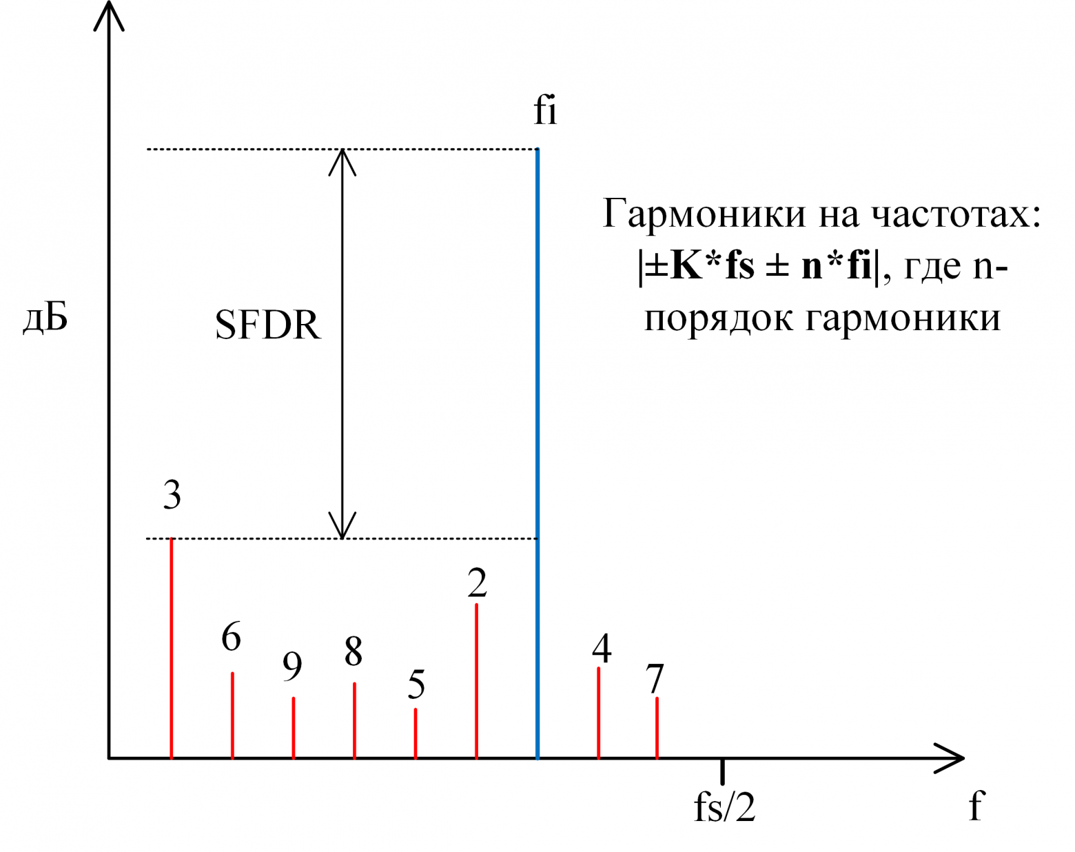
- Общие нелинейные искажения (THD — total harmonic distortion). Прежде, чем сигнал преобразовывается в цифровой код, он проходит через нелинейные блоки, которые искажают сигнал. К примеру, пусть есть сигнал с частотой f. Пройдя через нелинейный блок к нему добавятся компоненты с частотами 2f, 3f, 4f … — 2-я, 3-я, 4-я и т.д. гармоники входного сигнала. Если дискретизированный сигнал разложить в спектр с помощью ДПФ (Дискретного Преобразования Фурье), мы увидим, что все эти гармоники «перенеслись» в первую зону Найквиста (от 0 до fs/2) (рис. 9).
Рис. 9: Нелинейные искажения
Побочные гармоники искажают обрабатываемый сигнал, что ухудшает производительность системы. Этот эффект можно измерить, используя характеристику общие нелинейные искажения. THD определяется как отношение суммарной мощности гармонических частотных составляющих к мощности основной (исходной) частотной составляющей (в некоторых документациях выражается в дБ):
- Динамический диапазон, свободный от гармоник (SFDR — Spurious-Free Dynamic Range). Является отношением мощности полезного сигнала к мощности наибольшего «спура» (любая паразитная составляющая в спектре, не обязательно гармонического происхождения), присутствующего в спектре (рис. 9).
- Отношение сигнал / шум и нелинейные искажения (SINAD — signal-to-noise and distortion ratio). Аналогичен SNR, но помимо шума учитывает все виды помех и искажений, возникающих при аналого-цифровом преобразовании. SINAD является одним из ключевых параметром, характеризующим АЦП (в некоторых источниках обозначается как SNDR):
- Эффективное число бит (ENOB — effective number of bits) – некая абстрактная характеристика, показывающая сколько на самом деле бит в выходном коде АЦП несет в себе полезную информацию. Может принимать дробные значения.
- Интермодуляционные искажения (IMD — intermodulation distortion). Рассмотренные прежде динамические параметры измеряются, когда на вход подается однотональный гармонический сигнал. Такие однотональные тесты хороши, когда АЦП обрабатывает широкополосные сигналы. В этом случае гармоники, располагающиеся выше fs/2 отражаются в первую зону Найквиста и, следовательно, всегда учитываются в расчете параметров. Однако, имея дело с узкополосными сигналами или АЦП с передискретизацией, даже гармоники низкого порядка (2-я, 3-я) могут иметь достаточно высокую частоту, чтобы выйти из рассматриваемого частотного диапазона (или не отразиться в этот диапазон в случае выхода за fs/2). В этом случае эти гармоники не будут учтены, что приведёт к ошибочному завышению динамических параметров.
Для решения этой проблемы используются бигармонические тесты. На вход подают две спектрально чистых синусоиды одинаковой мощности с частотами и , которые находятся на близком расстоянии друг от друга. Нелинейность преобразователя порождает дополнительные тоны в спектре (их называют интермодуляционными искажениями) на частотах , где – произвольные целые числа.
Полезность бигармонического теста в том, что некоторые из интермодуляционных продуктов располагаются в спектре очень близко к исходному сигналу и, следовательно, дают полную информацию о нелинейности АЦП. В частности, интермодуляционные искажения 3-го порядка находятся на частотах и (рис. 10).
Рис. 10: интермодуляционные искажения
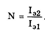
При построении РЧ систем могут быть интересны так же продукты 2-го и более высокого порядка. Параметр АЦП, характеризующий его интермодуляционные искажения n-го порядка, определяется формулой:
[dBc], где – мощность идентичных синусоид на входе, – мощность одного из продуктов. Например – отношение мощности на к мощности на


 и
и  , которые находятся на близком расстоянии друг от друга. Нелинейность преобразователя порождает дополнительные тоны в спектре (их называют интермодуляционными искажениями) на частотах
  , где
, где  – произвольные целые числа.
 и
и  (рис. 10).

 [dBc], где
  – мощность идентичных синусоид на входе,
  – мощность одного из продуктов. Например
  – отношение мощности на
Полоса пропускания АЦП и субдискретизация (undersamling/sub-sampling)
Полоса пропускания преобразователя (FPBW — Full Power (Analog) Bandwidth). Обычно ширина полосы преобразователя составляет несколько зон Найквиста. Этот параметр должен быть в спецификации, но, если его нет, можно попробовать самостоятельно оценить минимально возможное значение полосы пропускания для данного АЦП. За период выборки емкость УВХ должна зарядиться с точностью 1 LSB. Если период выборки равен  , то ошибка выборки сигнала полной шкалы равна:

Решив относительно t, получаем:

Положив, что  , определим минимальную полосу АЦП (для
  ):
):

Например, для 16 битного АЦП с частотой дискретизации 80 Мвыб/c и шкалой 2 В ограничение снизу для полосы пропускания, рассчитанное по этой формуле, составит FPBW = 282 МГц.
Analog Bandwidth является очень важным параметром при построении систем, которые работают в режиме субдискретизации (“undersampling”). Объясним это подробнее.
Согласно критерию Найквиста, ширина спектра обрабатываемого сигнала должна быть как минимум в 2 раза меньше частоты дискретизации, чтобы избежать элайзинга. Здесь важно, что именно ширина полосы, а не просто максимальная частота сигнала. Например, сигнал, спектр которого расположен целиком в 6-й зоне Найквиста может быть теоретически дискретизован без потери информации (рис. 11). Ограничив спектр этого сигнала антиэлайзинговым фильтром, его можно подавать на дискретизатор с частотой fs. В результате сигнал отразится в каждой зоне.
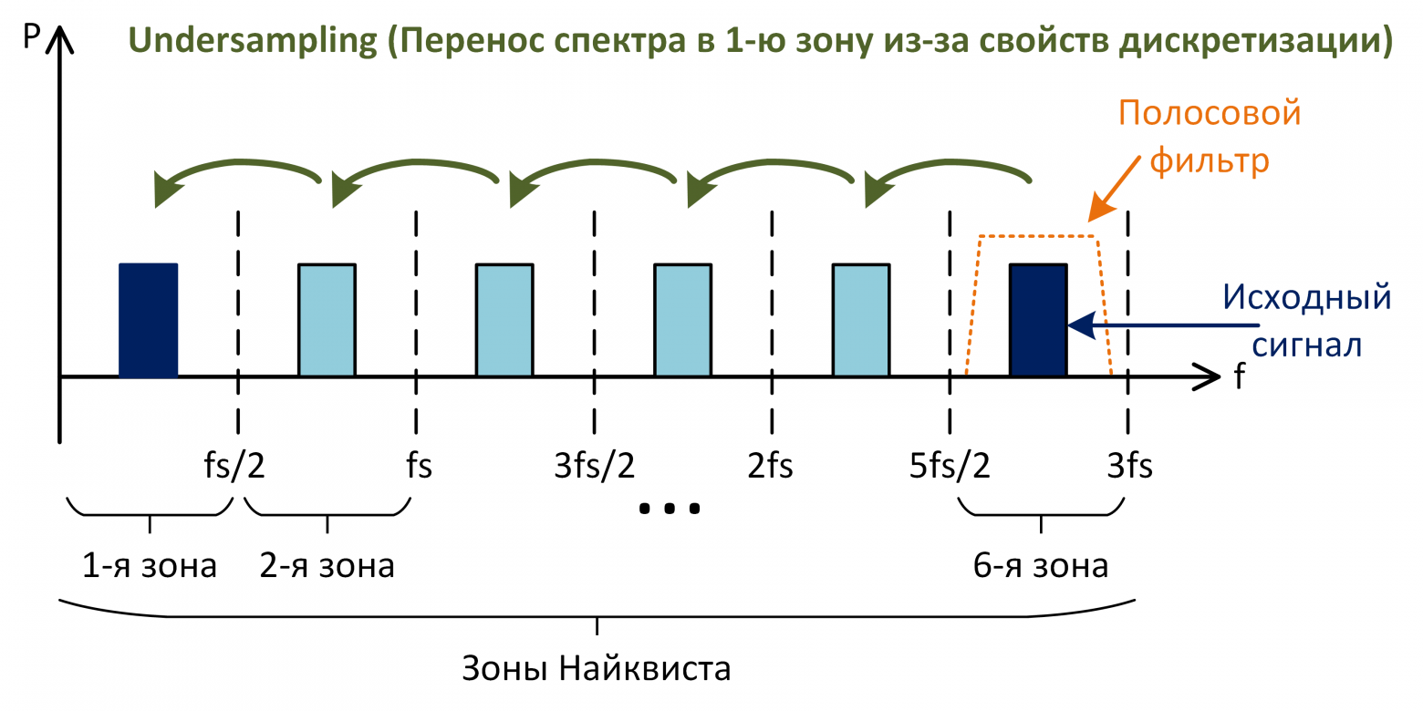
Рис. 11: undersampling
Свойство переноса спектра при дискретизации
Undersampling или sub-sampling имеет место быть из-за свойств дискретизации. Рассмотрим на примере, пусть имеется сигнал a(t) и его спектральная плотность  (рис. 12). Необходимо найти спектральную плотность
  сигнала после дискретизации сигнала
  .
.
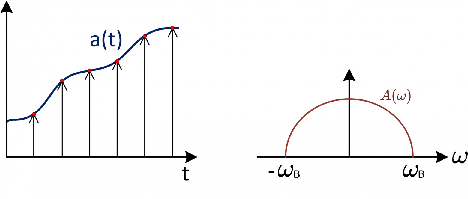
Рис 12: дискретизация непрерывного сигнала
По фильтрующему свойству дельта-функции:

После дискретизации  :
:

где 
С помощью формулы Релея вычислим спектр:


Из этого выражения следует что спектр сигнала будет повторяться во всех зонах Найквиста.
Итак, если есть хороший антиэлайзинговый фильтр, то соблюдая критерий Найквиста, можно оцифровывать сигнал с частотой дискретизации намного ниже полосы АЦП. Но использовать субдискретизацию нужно осторожно. Следует учитывать, что динамические параметры АЦП деградируют (иногда очень сильно) с ростом частоты входного сигнала, поэтому оцифровать сигнал из 6-й зоны так же «чисто», как из 1-й не получится.
Несмотря на это субдискритезация активно используется. Например, для обработки узкополосных сигналов, когда не хочется тратиться на дорогой широкополосный быстродействующий АЦП, который вдобавок имеет высокое потребление. Другой пример – выборка ПЧ (IF-sampling) в РЧ системах. Там благодаря undersampling можно исключить из радиоприемного тракта лишнее аналоговое звено — смеситель (который переносит сигнал на более низкую несущую или на 0).
Сравним архитектуры
На данный момент в мире существует множество различных архитектур АЦП. У каждой из них есть свои преимущества и недостатки. Не существует архитектуры, которая бы достигала максимальных значений всех, описанных выше параметров. Проанализируем какие максимальные параметры скорости и разрешения смогли достичь компании, выпускающие АЦП. Также оценим достоинства и недостатки каждой архитектуры (более подробно о различных архитектурах можно прочитать в статье на хабр).
Таблица сравнения архитектур
Информацию для таблицы брал на сайте arrow, поэтому если что-то упустил поправляйте в комментариях.
Заключение
Описав параметры разрабатываемой вами системы, можно понять, какие характеристики АЦП для вас являются критичными. Однако не стоит забывать, что динамические параметры преобразователей сильно зависят от многих факторов (частота дискретизации, частота входного сигнала, амплитуда входного сигнала и тд.) Зачастую в таблицах параметров в документации указывают только «красивые» (с точки зрения маркетинга) цифры. Приведу пример, возьмем АЦП ad9265 и рассмотрим его параметр SFDR при частоте входного сигнала 70 МГц:
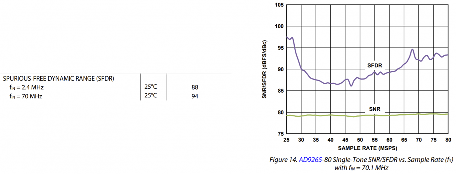
Таблица показывает значение SFDR при максимальных значениях частоты дискретизации, однако если вы будете использовать частоту ниже (к примеру 40 МГц), вы не получите этих «хороших» значений. Поэтому советую анализировать характеристики АЦП по графикам, чтобы примерно понимать, сможет ли данная микросхема обеспечить нужную вам точность преобразования.
26.
Принципы построения аналого-цифровых
преобразователей (AЦП).
Величина и знак ошибки квантования в
АЦП.
Аналого-цифровые
преобразователи (АЦП) – это устройства,
предназначенные для преобразования
аналоговых сигналов в цифровые. Для
такого преобразования необходимо
осуществить квантование аналогового
сигнала, т. е. мгновенные значения
аналогового сигнала ограничить
определенными уровнями, называемыми
уровнями квантования.
Характеристика
идеального квантования имеет вид,
приведенный на рис. 3.3.

Квантование
представляет собой округление аналоговой
величины до ближайшего уровня квантования,
т. е. максимальная погрешность квантования
равна ±0,5h (h – шаг квантования).
К
основным характеристикам АЦП относят
число разрядов, время преобразования,
нелинейность и др.
Число
разрядов – количество разрядов кода,
связанного с аналоговой величиной,
которое может вырабатывать АЦП. Часто
говорят о разрешающей способности АЦП,
которую определяют величиной, обратной
максимальному числу кодовых комбинаций
на выходе АЦП. Так, 10-разрядный АЦП имеет
разрешающую способность (210 = 1024)-1, т. е.
при шкале АЦП, соответствующей 10 В,
абсолютное значение шага квантования
не превышает 10 мВ. Время преобразования
tпр – интервал времени от момента
заданного изменения сигнала на входе
АЦП до появления на его выходе
соответствующего устойчивого кода.
Характерными
методами преобразования являются
следующие: параллельного преобразования
аналоговой величины и последовательного
преобразования.
АЦП
с двойным интегрированием реализует
также метод последовательного
преобразования входного сигнала (рис.
———————->). Использованы следующие
обозначения: СУ – система управления,
ГИ – генератор импульсов, Сч – счетчик
импульсов.
Принцип
действия АЦП
состоит в определении отношения двух
отрезков времени, в течение одного из
которых выполняется интегрирование
входного напряжения Uвх интегратором
на основе ОУ (напряжение Uи на выходе
интегратора изменяется от нуля до
максимальной по модулю величины), а в
течение следующего – интегрирование
опорного напряжения Uоп (Uи меняется от
максимальной по модулю величины до
нуля) (рис. 3.8). Пусть время t1 интегрирования
входного сигнала постоянно, тогда чем
больше второй отрезок времени t2 (отрезок
времени, в течение которого интегрируется
опорное напряжение), тем больше входное
напряжение. Ключ К3 предназначен для
установки интегратора в исходное нулевое
состояние. В первый из указанных отрезков
времени ключ К1 замкнут, ключ K2 разомкнут,
а во второй, отрезок времени их состояние
является обратным по отношению к
указанному. Одновременно с замыканием
ключа K2 импульсы с генератора импульсов
ГИ начинают поступать через схему
управления СУ на счетчик Сч. Поступление
этих импульсов заканчивается тогда,
когда напряжение на выходе интегратора
оказывается равным нулю. 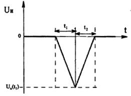
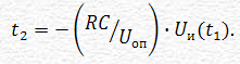
Напряжение
на выходе интегратора по истечении
отрезка времени t1
определяется выражением:

Используя
аналогичное выражение для отрезка
времени t2 получим:


Имеется
несколько источников погрешности АЦП.
Ошибки
квантования
и (считая, что АЦП должен быть линейным)
нелинейности присущи любому
аналого-цифровому преобразованию. Кроме
того, существуют так называемые апертурные
ошибки которые являются следствием
джиттера (англ. jitter) тактового генератора,
они проявляются при преобразовании
сигнала в целом (а не одного отсчёта).
Эти
ошибки измеряются в единицах, называемых
МЗР — младший значащий разряд. В
приведённом выше примере 8-битного
двоичного АЦП ошибка в 1 МЗР составляет
1/256 от полного диапазона сигнала, то
есть 0,4 %, в 5-тритном троичном АЦП ошибка
в 1 МЗР составляет 1/243 от полного диапазона
сигнала, то есть 0,412 %, в 8-тритном троичном
АЦП ошибка в 1 МЗР составляет 1/6561, то
есть 0,015 %.
Ошибки
квантования являются следствием
ограниченного разрешения АЦП. Этот
недостаток не может быть устранён ни
при каком типе аналого-цифрового
преобразования. Абсолютная величина
ошибки квантования при каждом отсчёте
находится в пределах от нуля до половины
МЗР.
Как
правило, амплитуда входного сигнала
много больше, чем МЗР. В этом случае
ошибка квантования не коррелирована с
сигналом и имеет равномерное распределение.
Её среднеквадратическое значение
совпадает с среднеквадратичным
отклонением распределения, которое
равно
 .
.
В случае 8-битного АЦП это составит 0,113
% от полного диапазона сигнала.
27.
Принцип работы цифроаналогового
преобразователя (ЦАП). Анализ работы
сигма-дельта модулятора. Линейная модель
сигма-дельта модулятора. Дискретизация
с перекрытием и формирование шума.
Функции передачи сигнала и шума в
линейной модели сигма — дельта модулятора.
АЦП с сигма-дельта модулятором первого
порядка.
Цифро-аналоговые
преобразователи (ЦАП) служат для
преобразования информации из цифровой
формы в аналоговый сигнал – суммирование
токов и напряжений. ЦАП широко применяется
в различных устройствах автоматики для
связи цифровых ЭВМ с аналоговыми
элементами и системами.
Принцип
работы ЦАП состоит в суммировании
аналоговых сигналов, пропорциональных
весам разрядов входного цифрового кода,
с коэффициентами, равными нулю или
единице в зависимости от значения
соответствующего разряда кода.
ЦАП
преобразует цифровой двоичный код
Q4Q3Q2Q1 в аналоговую величину, обычно
напряжение Uвых.. Каждый разряд двоичного
кода имеет определенный вес i-го разряда
вдвое больше, чем вес (i-1)-го. Работу ЦАП
можно описать следующей формулой:
![]()
где
e — напряжение, соответствующее весу
младшего разряда, Qi — значение i -го
разряда двоичного кода (0 или 1).
Например,
числу 1001 соответствует
![]()
Упрощенная
схема реализации ЦАП представлена на
рис1. В схеме i – й ключ замкнут при Qi=1,
при Qi=0 – разомкнут. Регистры подобраны
таким образом, что R>>Rн.
Рисунок
1. Схема ЦАП
Эквивалентное
сопротивление обведенного пунктиром
двухполюсника Rэк и сопротивление
нагрузки Rн образуют делитель напряжения,
тогда![]()
Проводимость
двухполюсника 1 / Rэк равна сумме
проводимостей ветвей (при Qi=1 i – ветвь
включена, при Qi=0 – отключена):


Очевидно,
что е = 8Е Rн / R. Выбором е можно установить
требуемый масштаб аналоговой величины.
АЦП
многотактного интегрирования имеют
ряд недостатков. Во-первых, нелинейность
переходной статической характеристики
операционного усилителя, на котором
выполняют интегратор, заметным образом
сказывается на интегральной нелинейности
характеристики преобразования АЦП
высокого разрешения. Для уменьшения
влияния этого фактора АЦП изготавливают
многотактными. Например, 13-разрядный
AD7550 выполняет преобразование в четыре
такта. Другим недостатком этих АЦП
является то обстоятельство, что
интегрирование входного сигнала занимает
в цикле преобразования только
приблизительно третью часть. Две трети
цикла преобразователь не принимает
входной сигнал. Это ухудшает
помехоподавляющие свойства интегрирующего
АЦП. В-третьих, АЦП многотактного
интегрирования должен быть снабжен
довольно большим количеством внешних
резисторов и конденсаторов с
высококачественным диэлектриком, что
значительно увеличивает место, занимаемое
преобразователем на плате и, как
следствие, усиливает влияние помех. 
Эти
недостатки во многом устранены в
конструкции сигма-дельта
АЦП
(в ранней литературе эти преобразователи
назывались АЦП с уравновешиванием или
балансом зарядов). Своим названием эти
преобразователи обязаны наличием в них
двух блоков: сумматора (обозначение
операции — S) и интегратора (обозначение
операции — D ). Один из принципов, заложенных
в такого рода преобразователях,
позволяющий уменьшить погрешность,
вносимую шумами, а следовательно
увеличить разрешающую способность —
это усреднение результатов измерения
на большом интервале времени. Основные
узлы АЦП — это сигма-дельта модулятор и
цифровой фильтр. Схема n-разрядного
сигма-дельта модулятора первого порядка
приведена на рис. 14. Работа этой схемы
основана на вычитании из входного
сигнала Uвх(t) величины сигнала на выходе
ЦАП, полученной на предыдущем такте
работы схемы. Полученная разность
интегрируется, а затем преобразуется
в код параллельным АЦП невысокой
разрядности. Последовательность кодов
поступает на цифровой фильтр нижних
частот. Порядок модулятора определяется
численностью интеграторов и сумматоров
в его схеме. Сигма-дельта модуляторы
N-го порядка содержат N сумматоров и N
интеграторов и обеспечивают большее
соотношение сигнал/шум при той же частоте
отсчетов, чем модуляторы первого порядка.
Примерами сигма-дельта модуляторов
высокого порядка являются одноканальный
AD7720 седьмого порядка и двухканальный
ADMOD79 пятого порядка.
Наиболее
широко в составе ИМС используются
однобитные сигма-дельта модуляторы, в
которых в качестве АЦП используется
компаратор, а в качестве ЦАП — аналоговый
комутатор (рис. 15). Принцип действия
пояснен в табл. 2 на примере преобразования
входного сигнала, равного 0,6 В, при Uоп=1
В. Пусть постоянная времени интегрирования
интегратора численно равна периоду
тактовых импульсов. В нулевом периоде
выходное напряжение интегратора
сбрасывается в нуль. На выходе ЦАП также
устанавливается нулевое напряжение. 
В
то же время применение цифрового фильтра
нижних частот в составе сигма-дельта
АЦП вместо счетчика вызывает переходные
процессы при изменении входного
напряжения. Время установления цифровых
фильтров с конечной длительностью
переходных процессов, как следует из
их названия, конечно и составляет для
фильтра вида (sinx/x)3 четыре периода частоты
отсчетов, а при начальном обнулении
фильтра — три периода. Это снижает
быстродействие систем сбора данных на
основе сигма-дельта АЦП. Поэтому
выпускаются ИМС AD7730 и AD7731, оснащенные
сложным цифровым фильтром, обеспечивающие
переключение каналов со временем
установления 1 мс при сохранении
эффективной разрядности не ниже 13 бит
(так называемый Fast-Step режим). Обычно
цифровой фильтр изготавливается на том
же кристалле, что и модулятор, но иногда
они выпускаются в виде двух отдельных
ИМС (например, AD1555 — модулятор четвертого
порядка и AD1556 — цифровой фильтр).
Сравнение
сигма-дельта АЦП с АЦП многотактного
интегрирования показывает значительные
преимущества первых. Прежде всего,
линейность характеристики преобразования
сигма-дельта АЦП выше, чем у АЦП
многотактного интегрирования равной
стоимости. Это объясняется тем, что
интегратор сигма-дельта АЦП работает
в значительно более узком динамическом
диапазоне, и нелинейность переходной
характеристики усилителя, на котором
построен интегратор, сказывается
значительно меньше. Емкость конденсатора
интегратора у сигма-дельта АЦП значительно
меньше (десятки пикофарад), так что этот
конденсатор может быть изготовлен прямо
на кристалле ИМС. Как следствие,
сигма-дельта АЦП практически не имеет
внешних элементов, что существенно
сокращает площадь, занимаемую им на
плате, и снижает уровень шумов. В
результате, например, 24-разрядный
сигма-дельта АЦП AD7714 изготавливается
в виде однокристалльной ИМС в 24-выводном
корпусе, потребляет 3 мВт мощности и
стоит примерно 14 долларов США, а
18-разрядный АЦП восьмитактного
интегрирования HI-7159 потребляет 75 мВт и
стоит около 30 долларов. К тому же
сигма-дельта АЦП начинает давать
правильный результат через 3-4 отсчета
после скачкообразного изменения входного
сигнала, что при величине первой частоты
режекции, равной 50 Гц, и 20-разрядном
разрешении составляет 60-80 мс, а минимальное
время преобразования АЦП HI-7159 для
18-разрядного разрешения и той же частоты
режекции составляет 140 мс. В настоящее
время ряд ведущих по аналого-цифровым
ИМС фирм, такие как Analog Devices и Burr-Brown,
прекратили производство АЦП многотактного
интегрирования, полностью перейдя в
области АЦ-преобразования высокого
разрешения на сигма-дельта АЦП.
Сигма-дельта
АЦП высокого разрешения имеют развитую
цифровую часть, включающую микроконтроллер.
Это позволяет реализовать режимы
автоматической установки нуля и
самокалибровки полной шкалы, хранить
калибровочные коэффициенты и передавать
их по запросу внешнего процессора.
28.
Транзисторные структуры (ТС).
Диодно-транзисторные структуры (ДТС)
как отражатели тока. Токовое зеркало
Уилсона. Биполярно-униполярные структуры.
Отражатели тока на ПТ.
При проектировании ПИС могут быть
получены АЭ с заданными свойствами, при
этом возможны два пути: схемотехнический
и конструкционный. При схемотехническом
подходе структуры АЭ получают путем
соединения различными способами
нескольких БТ (рис.1.1.а,в,ж), или БТ и ПТ,
образующие биполярно-униполярные(полевые)
структуры (рис.1.1.м,н), а также комбинации
БТ или ПТ с пассивными (резистивными)
элементами(рис.1.1. д,е,л), эквивалентные
одному БТ(рис.1.1.б,г) или одному ПТ(рис.1.1.о)
исходных типов, но с улучшенными
параметрами. К конструкционным ТС
относятся два и более БТ(рис1.1. з) или
ПТ, выполненные в едином технологическом
цикле производства на одной подложке
с идентичными параметрами, которые
существенно расширяют функциональные
возможности АЭ и позволяют использовать
их в качестве базовой схемы ДУ. Дискретные
варианты всех этих структур оказываются
неэффективными из-за нарушения принципа
идентичности характеристик отдельных
АЭ. При конструкционном подходе на
основе существующей технологии ПИС
создаются принципиально новые АЭ, не
имеющие аналогов в дискретном варианте:
например, многоэмиттерный n-p-n(рис.1.1.и)
или многоколлекторный p-n-p(рис.1.1.к)
БТ. Влияя на геометрические размеры
подобных ТС путем изменения площади
эмиттеров или коллекторов, можно получить
улучшенные технические характеристики
схем.

ДТС как
отражатели тока на БТ и ПТ. Разновидности
ДТС. Токовое зеркало Уилсона
Простейшая
ДТС(рис. а) содержит два идентичных БТ
с непосредственной связью эмиттеров,
причем один из транзисторов оказывается
прямосмещенным в диодном включении.
Исходя из
св-в идентичности характеристик БТ

(4.10)
отношение
токов I2/I1,
которое определяет коэффициент передачи
токов ДТС

Тогда
отношение токов

где N-
коэффициент отношения токов эмиттеров
БТ,входящих в ДТС
Если N=1,
то
При N=1
ДТС называется отражателем тока (токовым
зеркалом)
Более
совершенная ДТС (отражатель тока Уилсона)
строится на трех БТ(см. рис. е)

Соседние файлы в папке doc
- #
- #
- #
- #
- #
- #
- #
- #
- #
- #
- #
«A2D» redirects here. For the U.S. Navy attack aircraft, see Douglas A2D Skyshark.


In electronics, an analog-to-digital converter (ADC, A/D, or A-to-D) is a system that converts an analog signal, such as a sound picked up by a microphone or light entering a digital camera, into a digital signal. An ADC may also provide an isolated measurement such as an electronic device that converts an analog input voltage or current to a digital number representing the magnitude of the voltage or current. Typically the digital output is a two’s complement binary number that is proportional to the input, but there are other possibilities.
There are several ADC architectures. Due to the complexity and the need for precisely matched components, all but the most specialized ADCs are implemented as integrated circuits (ICs). These typically take the form of metal–oxide–semiconductor (MOS) mixed-signal integrated circuit chips that integrate both analog and digital circuits.
A digital-to-analog converter (DAC) performs the reverse function; it converts a digital signal into an analog signal.
Explanation[edit]
An ADC converts a continuous-time and continuous-amplitude analog signal to a discrete-time and discrete-amplitude digital signal. The conversion involves quantization of the input, so it necessarily introduces a small amount of quantization error. Furthermore, instead of continuously performing the conversion, an ADC does the conversion periodically, sampling the input, and limiting the allowable bandwidth of the input signal.
The performance of an ADC is primarily characterized by its bandwidth and signal-to-noise ratio (SNR). The bandwidth of an ADC is characterized primarily by its sampling rate. The SNR of an ADC is influenced by many factors, including the resolution, linearity and accuracy (how well the quantization levels match the true analog signal), aliasing and jitter. The SNR of an ADC is often summarized in terms of its effective number of bits (ENOB), the number of bits of each measure it returns that are on average not noise. An ideal ADC has an ENOB equal to its resolution. ADCs are chosen to match the bandwidth and required SNR of the signal to be digitized. If an ADC operates at a sampling rate greater than twice the bandwidth of the signal, then per the Nyquist–Shannon sampling theorem, near-perfect reconstruction is possible. The presence of quantization error limits the SNR of even an ideal ADC. However, if the SNR of the ADC exceeds that of the input signal, then the effects of quantization error may be neglected, resulting in an essentially perfect digital representation of the bandlimited analog input signal.
Resolution[edit]

The resolution of the converter indicates the number of different, i.e. discrete, values it can produce over the allowed range of analog input values. Thus a particular resolution determines the magnitude of the quantization error and therefore determines the maximum possible signal-to-noise ratio for an ideal ADC without the use of oversampling. The input samples are usually stored electronically in binary form within the ADC, so the resolution is usually expressed as the audio bit depth. In consequence, the number of discrete values available is usually a power of two. For example, an ADC with a resolution of 8 bits can encode an analog input to one in 256 different levels (28 = 256). The values can represent the ranges from 0 to 255 (i.e. as unsigned integers) or from −128 to 127 (i.e. as signed integer), depending on the application.
Resolution can also be defined electrically, and expressed in volts. The change in voltage required to guarantee a change in the output code level is called the least significant bit (LSB) voltage. The resolution Q of the ADC is equal to the LSB voltage. The voltage resolution of an ADC is equal to its overall voltage measurement range divided by the number of intervals:

where M is the ADC’s resolution in bits and EFSR is the full-scale voltage range (also called ‘span’). EFSR is given by

where VRefHi and VRefLow are the upper and lower extremes, respectively, of the voltages that can be coded.
Normally, the number of voltage intervals is given by

where M is the ADC’s resolution in bits.[1]
That is, one voltage interval is assigned in between two consecutive code levels.
Example:
- Coding scheme as in figure 1
- Full scale measurement range = 0 to 1 volt
- ADC resolution is 3 bits: 23 = 8 quantization levels (codes)
- ADC voltage resolution, Q = 1 V / 8 = 0.125 V.
In many cases, the useful resolution of a converter is limited by the signal-to-noise ratio (SNR) and other errors in the overall system expressed as an ENOB.
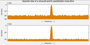
Quantization error[edit]

Quantization error is introduced by the quantization inherent in an ideal ADC. It is a rounding error between the analog input voltage to the ADC and the output digitized value. The error is nonlinear and signal-dependent. In an ideal ADC, where the quantization error is uniformly distributed between −1⁄2 LSB and +1⁄2 LSB, and the signal has a uniform distribution covering all quantization levels, the signal-to-quantization-noise ratio (SQNR) is given by
- [2]

where Q is the number of quantization bits. For example, for a 16-bit ADC, the quantization error is 96.3 dB below the maximum level.
Quantization error is distributed from DC to the Nyquist frequency. Consequently, if part of the ADC’s bandwidth is not used, as is the case with oversampling, some of the quantization error will occur out-of-band, effectively improving the SQNR for the bandwidth in use. In an oversampled system, noise shaping can be used to further increase SQNR by forcing more quantization error out of band.
Dither[edit]
In ADCs, performance can usually be improved using dither. This is a very small amount of random noise (e.g. white noise), which is added to the input before conversion. Its effect is to randomize the state of the LSB based on the signal. Rather than the signal simply getting cut off altogether at low levels, it extends the effective range of signals that the ADC can convert, at the expense of a slight increase in noise. Dither can only increase the resolution of a sampler. It cannot improve the linearity, and thus accuracy does not necessarily improve.
Quantization distortion in an audio signal of very low level with respect to the bit depth of the ADC is correlated with the signal and sounds distorted and unpleasant. With dithering, the distortion is transformed into noise. The undistorted signal may be recovered accurately by averaging over time. Dithering is also used in integrating systems such as electricity meters. Since the values are added together, the dithering produces results that are more exact than the LSB of the analog-to-digital converter.
Dither is often applied when quantizing photographic images to a fewer number of bits per pixel—the image becomes noisier but to the eye looks far more realistic than the quantized image, which otherwise becomes banded. This analogous process may help to visualize the effect of dither on an analog audio signal that is converted to digital.
Accuracy[edit]
An ADC has several sources of errors. Quantization error and (assuming the ADC is intended to be linear) non-linearity are intrinsic to any analog-to-digital conversion. These errors are measured in a unit called the least significant bit (LSB). In the above example of an eight-bit ADC, an error of one LSB is 1⁄256 of the full signal range, or about 0.4%.
Nonlinearity[edit]
All ADCs suffer from nonlinearity errors caused by their physical imperfections, causing their output to deviate from a linear function (or some other function, in the case of a deliberately nonlinear ADC) of their input. These errors can sometimes be mitigated by calibration, or prevented by testing. Important parameters for linearity are integral nonlinearity and differential nonlinearity. These nonlinearities introduce distortion that can reduce the signal-to-noise ratio performance of the ADC and thus reduce its effective resolution.
Jitter[edit]
When digitizing a sine wave  , the use of a non-ideal sampling clock will result in some uncertainty in when samples are recorded. Provided that the actual sampling time uncertainty due to clock jitter is
  , the error caused by this phenomenon can be estimated as
  . This will result in additional recorded noise that will reduce the effective number of bits (ENOB) below that predicted by quantization error alone. The error is zero for DC, small at low frequencies, but significant with signals of high amplitude and high frequency. The effect of jitter on performance can be compared to quantization error:
  , where q is the number of ADC bits.[citation needed]
| Output size (bits) |
Signal Frequency | ||||||
|---|---|---|---|---|---|---|---|
| 1 Hz | 1 kHz | 10 kHz | 1 MHz | 10 MHz | 100 MHz | 1 GHz | |
| 8 | 1,243 µs | 1.24 µs | 124 ns | 1.24 ns | 124 ps | 12.4 ps | 1.24 ps |
| 10 | 311 µs | 311 ns | 31.1 ns | 311 ps | 31.1 ps | 3.11 ps | 0.31 ps |
| 12 | 77.7 µs | 77.7 ns | 7.77 ns | 77.7 ps | 7.77 ps | 0.78 ps | 0.08 ps («77.7fs») |
| 14 | 19.4 µs | 19.4 ns | 1.94 ns | 19.4 ps | 1.94 ps | 0.19 ps | 0.02 ps («19.4fs») |
| 16 | 4.86 µs | 4.86 ns | 486 ps | 4.86 ps | 0.49 ps | 0.05 ps («48.5 fs») | – |
| 18 | 1.21 µs | 1.21 ns | 121 ps | 1.21 ps | 0.12 ps | – | – |
| 20 | 304 ns | 304 ps | 30.4 ps | 0.30 ps («303.56 fs») | 0.03 ps («30.3 fs») | – | – |
| 24 | 18.9 ns | 18.9 ps | 1.89 ps | 0.019 ps («18.9 fs») | — | – | – |
Clock jitter is caused by phase noise.[3][4] The resolution of ADCs with a digitization bandwidth between 1 MHz and 1 GHz is limited by jitter.[5] For lower bandwidth conversions such as when sampling audio signals at 44.1 kHz, clock jitter has a less significant impact on performance.[6]
Sampling rate[edit]
An analog signal is continuous in time and it is necessary to convert this to a flow of digital values. It is therefore required to define the rate at which new digital values are sampled from the analog signal. The rate of new values is called the sampling rate or sampling frequency of the converter. A continuously varying bandlimited signal can be sampled and then the original signal can be reproduced from the discrete-time values by a reconstruction filter. The Nyquist–Shannon sampling theorem implies that a faithful reproduction of the original signal is only possible if the sampling rate is higher than twice the highest frequency of the signal.
Since a practical ADC cannot make an instantaneous conversion, the input value must necessarily be held constant during the time that the converter performs a conversion (called the conversion time). An input circuit called a sample and hold performs this task—in most cases by using a capacitor to store the analog voltage at the input, and using an electronic switch or gate to disconnect the capacitor from the input. Many ADC integrated circuits include the sample and hold subsystem internally.
Aliasing[edit]
An ADC works by sampling the value of the input at discrete intervals in time. Provided that the input is sampled above the Nyquist rate, defined as twice the highest frequency of interest, then all frequencies in the signal can be reconstructed. If frequencies above half the Nyquist rate are sampled, they are incorrectly detected as lower frequencies, a process referred to as aliasing. Aliasing occurs because instantaneously sampling a function at two or fewer times per cycle results in missed cycles, and therefore the appearance of an incorrectly lower frequency. For example, a 2 kHz sine wave being sampled at 1.5 kHz would be reconstructed as a 500 Hz sine wave.
To avoid aliasing, the input to an ADC must be low-pass filtered to remove frequencies above half the sampling rate. This filter is called an anti-aliasing filter, and is essential for a practical ADC system that is applied to analog signals with higher frequency content. In applications where protection against aliasing is essential, oversampling may be used to greatly reduce or even eliminate it.
Although aliasing in most systems is unwanted, it can be exploited to provide simultaneous down-mixing of a band-limited high-frequency signal (see undersampling and frequency mixer). The alias is effectively the lower heterodyne of the signal frequency and sampling frequency.[7]
Oversampling[edit]
For economy, signals are often sampled at the minimum rate required with the result that the quantization error introduced is white noise spread over the whole passband of the converter. If a signal is sampled at a rate much higher than the Nyquist rate and then digitally filtered to limit it to the signal bandwidth produces the following advantages:
- Oversampling can make it easier to realize analog anti-aliasing filters
- Improved audio bit depth
- Reduced noise, especially when noise shaping is employed in addition to oversampling.
Oversampling is typically used in audio frequency ADCs where the required sampling rate (typically 44.1 or 48 kHz) is very low compared to the clock speed of typical transistor circuits (>1 MHz). In this case, the performance of the ADC can be greatly increased at little or no cost. Furthermore, as any aliased signals are also typically out of band, aliasing can often be eliminated using very low cost filters.
Relative speed and precision[edit]
The speed of an ADC varies by type. The Wilkinson ADC is limited by the clock rate which is processable by current digital circuits. For a successive-approximation ADC, the conversion time scales with the logarithm of the resolution, i.e. the number of bits. Flash ADCs are certainly the fastest type of the three; The conversion is basically performed in a single parallel step.
There is a potential tradeoff between speed and precision. Flash ADCs have drifts and uncertainties associated with the comparator levels results in poor linearity. To a lesser extent, poor linearity can also be an issue for successive-approximation ADCs. Here, nonlinearity arises from accumulating errors from the subtraction processes. Wilkinson ADCs have the best linearity of the three.[8][9]
Sliding scale principle[edit]
The sliding scale or randomizing method can be employed to greatly improve the linearity of any type of ADC, but especially flash and successive approximation types. For any ADC the mapping from input voltage to digital output value is not exactly a floor or ceiling function as it should be. Under normal conditions, a pulse of a particular amplitude is always converted to the same digital value. The problem lies in that the ranges of analog values for the digitized values are not all of the same widths, and the differential linearity decreases proportionally with the divergence from the average width. The sliding scale principle uses an averaging effect to overcome this phenomenon. A random, but known analog voltage is added to the sampled input voltage. It is then converted to digital form, and the equivalent digital amount is subtracted, thus restoring it to its original value. The advantage is that the conversion has taken place at a random point. The statistical distribution of the final levels is decided by a weighted average over a region of the range of the ADC. This in turn desensitizes it to the width of any specific level.[10][11]
Types[edit]
These are several common ways of implementing an electronic ADC.
RC charge time[edit]
Resistor-capacitor (RC) circuits have a known voltage charging and discharging curve that can be used to solve for an unknown analog value.
Wilkinson[edit]
The Wilkinson ADC was designed by Denys Wilkinson in 1950. The Wilkinson ADC is based on the comparison of an input voltage with that produced by a charging capacitor. The capacitor is allowed to charge until a comparator determines it matches the input voltage. Then, the capacitor is discharged linearly by using a constant current source. The time required to discharge the capacitor is proportional to the amplitude of the input voltage. While the capacitor is discharging, pulses from a high-frequency oscillator clock are counted by a register. The number of clock pulses recorded in the register is also proportional to the input voltage.[12][13]
Measuring analog resistance or capacitance[edit]
If the analog value to measure is represented by a resistance or capacitance, then by including that element in an RC circuit (with other resistances or capacitances fixed) and measuring the time to charge the capacitance from a known starting voltage to another known ending voltage through the resistance from a known voltage supply, the value of the unknown resistance or capacitance can be determined using the capacitor charging equation:

and solving for the unknown resistance or capacitance using those starting and ending datapoints. This is similar but contrasts to the Wilkinson ADC which measures an unknown voltage with a known resistance and capacitance, by instead measuring an unknown resistance or capacitance with a known voltage.
For example, the positive (and/or negative) pulse width from a 555 Timer IC in monostable or astable mode represents the time it takes to charge (and/or discharge) its capacitor from 1⁄3 Vsupply to 2⁄3 Vsupply. By sending this pulse into a microcontroller with an accurate clock, the duration of the pulse can be measured and converted using the capacitor charging equation to produce the value of the unknown resistance or capacitance.
Larger resistances and capacitances will take a longer time to measure than smaller one. And the accuracy is limited by the accuracy of the microcontroller clock and the amount of time available to measure the value, which potentially might even change during measurement or be affected by external parasitics.
Direct-conversion[edit]
A direct-conversion or flash ADC has a bank of comparators sampling the input signal in parallel, each firing for a specific voltage range. The comparator bank feeds a digital encoder logic circuit that generates a binary number on the output lines for each voltage range.
ADCs of this type have a large die size and high power dissipation. They are often used for video, wideband communications, or other fast signals in optical and magnetic storage.
The circuit consists of a resistive divider network, a set of op-amp comparators and a priority encoder. A small amount of hysteresis is built into the comparator to resolve any problems at voltage boundaries. At each node of the resistive divider, a comparison voltage is available. The purpose of the circuit is to compare the analog input voltage with each of the node voltages.
The circuit has the advantage of high speed as the conversion takes place simultaneously rather than sequentially. Typical conversion time is 100 ns or less. Conversion time is limited only by the speed of the comparator and of the priority encoder. This type of ADC has the disadvantage that the number of comparators required almost doubles for each added bit. Also, the larger the value of n, the more complex is the priority encoder.
Successive approximation[edit]
A successive-approximation ADC uses a comparator and a binary search to successively narrow a range that contains the input voltage. At each successive step, the converter compares the input voltage to the output of an internal digital-to-analog converter (DAC) which initially represents the midpoint of the allowed input voltage range. At each step in this process, the approximation is stored in a successive approximation register (SAR) and the output of the digital-to-analog converter is updated for a comparison over a narrower range.
Ramp-compare[edit]
A ramp-compare ADC produces a saw-tooth signal that ramps up or down then quickly returns to zero.[14]
When the ramp starts, a timer starts counting. When the ramp voltage matches the input, a comparator fires, and the timer’s value is recorded. Timed ramp converters can be implemented economically,[a] however, the ramp time may be sensitive to temperature because the circuit generating the ramp is often a simple analog integrator. A more accurate converter uses a clocked counter driving a DAC. A special advantage of the ramp-compare system is that converting a second signal just requires another comparator and another register to store the timer value. To reduce sensitivity to input changes during conversion, a sample and hold can charge a capacitor with the instantaneous input voltage and the converter can time the time required to discharge with a constant current.
Integrating[edit]
An integrating ADC (also dual-slope or multi-slope ADC) applies the unknown input voltage to the input of an integrator and allows the voltage to ramp for a fixed time period (the run-up period). Then a known reference voltage of opposite polarity is applied to the integrator and is allowed to ramp until the integrator output returns to zero (the run-down period). The input voltage is computed as a function of the reference voltage, the constant run-up time period, and the measured run-down time period. The run-down time measurement is usually made in units of the converter’s clock, so longer integration times allow for higher resolutions. Likewise, the speed of the converter can be improved by sacrificing resolution. Converters of this type (or variations on the concept) are used in most digital voltmeters for their linearity and flexibility.
- Charge balancing ADC
- The principle of charge balancing ADC is to first convert the input signal to a frequency using a voltage-to-frequency converter. This frequency is then measured by a counter and converted to an output code proportional to the analog input. The main advantage of these converters is that it is possible to transmit frequency even in a noisy environment or in isolated form. However, the limitation of this circuit is that the output of the voltage-to-frequency converter depends upon an RC product whose value cannot be accurately maintained over temperature and time.
- Dual-slope ADC
- The analog part of the circuit consists of a high input impedance buffer, precision integrator and a voltage comparator. The converter first integrates the analog input signal for a fixed duration and then it integrates an internal reference voltage of opposite polarity until the integrator output is zero. The main disadvantage of this circuit is the long duration time. They are particularly suitable for accurate measurement of slowly varying signals such as thermocouples and weighing scales.
Delta-encoded[edit]
A delta-encoded or counter-ramp ADC has an up-down counter that feeds a DAC. The input signal and the DAC both go to a comparator. The comparator controls the counter. The circuit uses negative feedback from the comparator to adjust the counter until the DAC’s output matches the input signal and number is read from the counter. Delta converters have very wide ranges and high resolution, but the conversion time is dependent on the input signal behavior, though it will always have a guaranteed worst-case. Delta converters are often very good choices to read real-world signals as most signals from physical systems do not change abruptly. Some converters combine the delta and successive approximation approaches; this works especially well when high frequency components of the input signal are known to be small in magnitude.
Pipelined[edit]
A pipelined ADC (also called subranging quantizer) uses two or more conversion steps. First, a coarse conversion is done. In a second step, the difference to the input signal is determined with a DAC. This difference is then converted more precisely, and the results are combined in the last step. This can be considered a refinement of the successive-approximation ADC wherein the feedback reference signal consists of the interim conversion of a whole range of bits (for example, four bits) rather than just the next-most-significant bit. By combining the merits of the successive approximation and flash ADCs this type is fast, has a high resolution, and can be implemented efficiently.
Delta-sigma[edit]
A delta-sigma ADC (also known as a sigma-delta ADC) is based on a negative feedback loop with an analog filter and low resolution (often 1 bit), but high-speed ADC and DAC to approximate the incoming signal. The filter (usually a 2nd order low pass filter) in the loop performs noise shaping: the quantization noise originating from the DAC is no longer evenly distributed over the frequencies, but higher for the high frequencies and reduced for the low frequencies.
A digital filter (decimation filter) then removes much of the higher frequencies (especially much of the quantization noise) and converts the data stream from high sampling rate and low resolution to low speed and high resolution.
Time-interleaved[edit]
A time-interleaved ADC uses M parallel ADCs where each ADC samples data every M:th cycle of the effective sample clock. The result is that the sample rate is increased M times compared to what each individual ADC can manage. In practice, the individual differences between the M ADCs degrade the overall performance reducing the spurious-free dynamic range (SFDR).[16] However, techniques exist to correct for these time-interleaving mismatch errors.[17]
Intermediate FM stage[edit]
An ADC with an intermediate FM stage first uses a voltage-to-frequency converter to produce an oscillating signal with a frequency proportional to the voltage of the input signal, and then uses a frequency counter to convert that frequency into a digital count proportional to the desired signal voltage. Longer integration times allow for higher resolutions. Likewise, the speed of the converter can be improved by sacrificing resolution. The two parts of the ADC may be widely separated, with the frequency signal passed through an opto-isolator or transmitted wirelessly. Some such ADCs use sine wave or square wave frequency modulation; others use pulse-frequency modulation. Such ADCs were once the most popular way to show a digital display of the status of a remote analog sensor.[18][19][20][21][22]
Time-stretch[edit]
A Time-stretch analog-to-digital converter (TS-ADC) digitizes a very wide bandwidth analog signal, that cannot be digitized by a conventional electronic ADC, by time-stretching the signal prior to digitization. It commonly uses a photonic preprocessor to time-stretch the signal, which effectively slows the signal down in time and compresses its bandwidth. As a result, an electronic ADC, that would have been too slow to capture the original signal, can now capture this slowed-down signal. For continuous capture of the signal, the front end also divides the signal into multiple segments in addition to time-stretching. Each segment is individually digitized by a separate electronic ADC. Finally, a digital signal processor rearranges the samples and removes any distortions added by the preprocessor to yield the binary data that is the digital representation of the original analog signal.
Commercial[edit]
In many cases, the most expensive part of an integrated circuit is the pins, because they make the package larger, and each pin has to be connected to the integrated circuit’s silicon. To save pins, it is common for ADCs to send their data one bit at a time over a serial interface to the computer, with each bit coming out when a clock signal changes state. This saves quite a few pins on the ADC package, and in many cases, does not make the overall design any more complex.
Commercial ADCs often have several inputs that feed the same converter, usually through an analog multiplexer. Different models of ADC may include sample and hold circuits, instrumentation amplifiers or differential inputs, where the quantity measured is the difference between two inputs.
Applications[edit]
Music recording[edit]
Analog-to-digital converters are integral to modern music reproduction technology and digital audio workstation-based sound recording. Music may be produced on computers using an analog recording and therefore analog-to-digital converters are needed to create the pulse-code modulation (PCM) data streams that go onto compact discs and digital music files. The current crop of analog-to-digital converters utilized in music can sample at rates up to 192 kilohertz. Many recording studios record in 24-bit 96 kHz pulse-code modulation (PCM) format and then downsample and dither the signal for Compact Disc Digital Audio production (44.1 kHz) or to 48 kHz for radio and television broadcast applications.
Digital signal processing[edit]
ADCs are required in digital signal processing systems that process, store, or transport virtually any analog signal in digital form. TV tuner cards, for example, use fast video analog-to-digital converters. Slow on-chip 8-, 10-, 12-, or 16-bit analog-to-digital converters are common in microcontrollers. Digital storage oscilloscopes need very fast analog-to-digital converters, also crucial for software-defined radio and their new applications.
Scientific instruments[edit]
Digital imaging systems commonly use analog-to-digital converters for digitizing pixels. Some radar systems use analog-to-digital converters to convert signal strength to digital values for subsequent signal processing. Many other in situ and remote sensing systems commonly use analogous technology.
Many sensors in scientific instruments produce an analog signal; temperature, pressure, pH, light intensity etc. All these signals can be amplified and fed to an ADC to produce a digital representation.
Rotary encoder[edit]
Some non-electronic or only partially electronic devices, such as rotary encoders, can also be considered ADCs. Typically the digital output of an ADC will be a two’s complement binary number that is proportional to the input. An encoder might output a Gray code.
Displays[edit]
Flat-panel displays are inherently digital and need an ADC to process an analog signal such as composite or VGA.
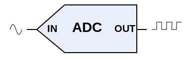
Electrical symbol[edit]
Testing[edit]
Testing an analog-to-digital converter requires an analog input source and hardware to send control signals and capture digital data output. Some ADCs also require an accurate source of reference signal.
The key parameters to test an ADC are:
- DC offset error
- DC gain error
- signal-to-noise ratio (SNR)
- Total harmonic distortion (THD)
- Integral nonlinearity (INL)
- Differential nonlinearity (DNL)
- Spurious free dynamic range
- Power dissipation
See also[edit]
- Adaptive predictive coding, a type of ADC in which the value of the signal is predicted by a linear function
- Audio codec
- Beta encoder
- Integral linearity
- Modem
Notes[edit]
- ^ A very simple (nonlinear) ramp converter can be implemented with a microcontroller and one resistor and capacitor.[15]
References[edit]
- ^ «Principles of Data Acquisition and Conversion» (PDF). Texas Instruments. April 2015. Archived (PDF) from the original on October 9, 2022. Retrieved October 18, 2016.
- ^ Lathi, B.P. (1998). Modern Digital and Analog Communication Systems (3rd ed.). Oxford University Press.
- ^ «Maxim App 800: Design a Low-Jitter Clock for High-Speed Data Converters», maxim-ic.com, July 17, 2002
- ^ «Jitter effects on Analog to Digital and Digital to Analog Converters» (PDF). Retrieved August 19, 2012.
- ^ Löhning, Michael; Fettweis, Gerhard (2007). «The effects of aperture jitter and clock jitter in wideband ADCs». Computer Standards & Interfaces Archive. 29 (1): 11–18. CiteSeerX 10.1.1.3.9217. doi:10.1016/j.csi.2005.12.005.
- ^ Redmayne, Derek; Steer, Alison (December 8, 2008), «Understanding the effect of clock jitter on high-speed ADCs», eetimes.com
- ^ «RF-Sampling and GSPS ADCs – Breakthrough ADCs Revolutionize Radio Architectures» (PDF). Texas Instruments. Archived (PDF) from the original on October 9, 2022. Retrieved November 4, 2013.
- ^ Knoll (1989, pp. 664–665)
- ^ Nicholson (1974, pp. 313–315)
- ^ Knoll (1989, pp. 665–666)
- ^ Nicholson (1974, pp. 315–316)
- ^ Knoll (1989, pp. 663–664)
- ^ Nicholson (1974, pp. 309–310)
- ^ Couch — 2001 — Digital and analog communication systems — Prentice Hall — New Jersey, USA
- ^ «Atmel Application Note AVR400: Low Cost A/D Converter» (PDF). atmel.com. Archived (PDF) from the original on October 9, 2022.
- ^ Vogel, Christian (2005). «The Impact of Combined Channel Mismatch Effects in Time-interleaved ADCs». IEEE Transactions on Instrumentation and Measurement. 55 (1): 415–427. CiteSeerX 10.1.1.212.7539. doi:10.1109/TIM.2004.834046. S2CID 15038020.
- ^ Gabriele Manganaro; David H. Robertson (July 2015), Interleaving ADCs: Unraveling the Mysteries, Analog Devices, retrieved October 7, 2021
- ^
Analog Devices MT-028 Tutorial: «Voltage-to-Frequency Converters» by Walt Kester and James Bryant 2009,
apparently adapted from Kester, Walter Allan (2005) Data conversion handbook, Newnes, p. 274, ISBN 0750678410. - ^
Microchip AN795 «Voltage to Frequency / Frequency to Voltage Converter» p. 4: «13-bit A/D converter» - ^ Carr, Joseph J. (1996) Elements of electronic instrumentation and measurement, Prentice Hall, p. 402, ISBN 0133416860.
- ^ «Voltage-to-Frequency Analog-to-Digital Converters». globalspec.com
- ^ Pease, Robert A. (1991) Troubleshooting Analog Circuits, Newnes, p. 130, ISBN 0750694998.
- Knoll, Glenn F. (1989). Radiation Detection and Measurement (2nd ed.). New York: John Wiley & Sons. ISBN 978-0471815044.
- Nicholson, P. W. (1974). Nuclear Electronics. New York: John Wiley & Sons. pp. 315–316. ISBN 978-0471636977.
Further reading[edit]
- Allen, Phillip E.; Holberg, Douglas R. (2002). CMOS Analog Circuit Design. ISBN 978-0-19-511644-1.
- Fraden, Jacob (2010). Handbook of Modern Sensors: Physics, Designs, and Applications. Springer. ISBN 978-1441964656.
- Kester, Walt, ed. (2005). The Data Conversion Handbook. Elsevier: Newnes. ISBN 978-0-7506-7841-4.
- Johns, David; Martin, Ken (1997). Analog Integrated Circuit Design. ISBN 978-0-471-14448-9.
- Liu, Mingliang (2006). Demystifying Switched-Capacitor Circuits. ISBN 978-0-7506-7907-7.
- Norsworthy, Steven R.; Schreier, Richard; Temes, Gabor C. (1997). Delta-Sigma Data Converters. IEEE Press. ISBN 978-0-7803-1045-2.
- Razavi, Behzad (1995). Principles of Data Conversion System Design. New York, NY: IEEE Press. ISBN 978-0-7803-1093-3.
- Ndjountche, Tertulien (May 24, 2011). CMOS Analog Integrated Circuits: High-Speed and Power-Efficient Design. Boca Raton, FL: CRC Press. ISBN 978-1-4398-5491-4.
- Staller, Len (February 24, 2005). «Understanding analog to digital converter specifications». Embedded Systems Design.
- Walden, R. H. (1999). «Analog-to-digital converter survey and analysis». IEEE Journal on Selected Areas in Communications. 17 (4): 539–550. CiteSeerX 10.1.1.352.1881. doi:10.1109/49.761034.
External links[edit]
- An Introduction to Delta Sigma Converters A very nice overview of Delta-Sigma converter theory.
- Digital Dynamic Analysis of A/D Conversion Systems through Evaluation Software based on FFT/DFT Analysis RF Expo East, 1987
- Which ADC Architecture Is Right for Your Application? article by Walt Kester
- ADC and DAC Glossary at the Wayback Machine (archived 2009-11-24) Defines commonly used technical terms
- Introduction to ADC in AVR – Analog to digital conversion with Atmel microcontrollers
- Signal processing and system aspects of time-interleaved ADCs
- MATLAB Simulink model of a simple ramp ADC