Resources
PCB Design
Footprint Not Found? How to Find Missing Footprints
Created: January 26, 2017
Updated: March 16, 2020
Altium Designer — PCB Design Software
Altium 365 — PCB Design Platform
Enterprise PCB Design Solutions
FREE Trials
Related Resources

Risk Vs. Reward
During the recent IPC APEX expo, there was a lot of discussion about SAP, or semi-additive PCB processes. As with any new technology in PCB manufacturing, there were people that are excited to jump right in and start designing with much finer feature sizes and work through the inevitable changes to the traditional thought process. Others are in a let’s wait and see mode and of course, there are a few skeptics there as well. There were a few stand
Read Article

Build Your Own Laser Range Finder
Raspberry Pi Pico (RP2040) is a cute piece of hardware. It is equipped with a powerful dual-core RP2040 microcontroller that offers 2M (up to 16M) Flash and 264K SRAM memories. Such specifications for an MCU make it suitable for a variety of hobby and industrial applications. In this article, I used an RP2040 Zero board, a VL53L0X Laser time-of-flight ranging sensor, and a 2.4” TFT display to build a graphical laser rangefinder unit that can be
Read Article

LLC Resonant Converter Design and PCB Layout
You can use an LLC resonant converter design to provide stable DC power in your circuits. Here’s how to layout your LLC converter design.
Read Article

Grooming the Next Generation of Electronic Designers
Learn about Altium’s commitment to advancing electronic design when it comes to the next generation!
Read Article

Take the Risk Out of Prototype PCB Assembly (PCBA)
Take the risk out of your PCB assembly (PCBA) with supply chain management. There is a special feeling one gets when polishing off a Rev A design and ordering the first set of PCBs from a board house. While designers everywhere would likely not trade that feeling for anything, taking some of the uneasiness off the table would probably be a welcome change. Here are review steps that should prove more effective at settling nerves than an after-work
Read Article

Image Processing Embedded Systems with Modular Hardware
Image processing embedded systems can be deployed quickly thanks to modular design tools With advances in industrial automation, automotive technology, remote sensing, and much more, image processing is taking center stage in many embedded systems. Image processing with older video systems was difficult or impossible due to the low quality of many imaging systems with perpetual uptime. As a result, older camera systems could be developed for
Read Article

Can You Hear Me Now?
Depending on your background and personal experiences, two things may spring to mind when you hear the term “cocktail party problem.” The first is you thinking, “there are never enough cocktails to satisfy everyone’s requirements,” but maybe I’m projecting again. Alternatively, you may be considering how difficult it is for an artificial intelligence (AI)-enabled voice-controlled assistant like Amazon’s Alexa to follow individual voices when a
Read Article

Newer PCB Materials
If you are hearing about the newer, higher density HDI-PCBs used by Apple called SLP, and their processes like SAP, or uSAP or mSAP (Semi-Additive Processes) recently, these are the printed circuits that are getting down to 30 micron and 25 micron (1 mil) traces and spaces. HDI is now estimated to be over 250 million square meters produced per year-and still growing! But SAP is not NEW! We used it early in the 60’s and 70’s when we were making
Read Article

Clearing Up Trace Impedance Calculators and Formulas
While it might not be obvious to the casual or to those who think the mathematics underlying PCB design is largely settled, there is plenty of disagreement regarding the right formula to calculate trace impedance. This disagreement extends to online trace impedance calculators, and designers should make themselves aware of the limitations of these tools. The Problem with a Trace Impedance Calculator If you use your favorite search engine to find
Read Article
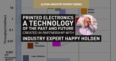
Printed Electronics a Technology of the Past and Future
Printed electronics (PE) is a new, rapidly growing interconnect business. It has its origin in printed-flexible keyboards for appliances and for the expanding technologies in fancy magazines and literature. The irony of PE is that the technology was probably the first employed during WWII and all printed circuits owes it origin to PE. APPLICATIONS The most exciting thing about PE is all the new applications and markets that it will open. In
Read Article
Back to Home
Try Altium Designer
Get Altium Designer for free for 2 weeks
Get Altium Designer for free for 2 weeks
Эта тема
- Везде
-
- Эта тема
- Этот форум
-
- Расширенный поиск
Поиск

Topic: Altium Library footprint not found [SOLVED] (Read 13243 times)
0 Members and 1 Guest are viewing this topic.
So i’m moving my MySQL database from AD16 to AD19.
I’ve got my DBLib up and running, coupled and everything.
When i browse my library in components, everything comes into view. So Schematic gets rendered, Footprint also.
I’ve updated the components in my schematic from my library, everything imported great.
When i try to import them in the PcbDoc -> Failed to add component class.
So take im taking a look at the component itself, looking at the properties.
The footprint is coupled, id is coupled, footprint is found.
Except, when i click on the edit footprint it says that the footprint is not found.
Anyone knowing what this issue is about ?
My paths do not contain spaces.. I’m scratching my head here..
« Last Edit: June 03, 2019, 10:32:48 pm by Ribster »

Logged
Ok, this is due to the table name changing.
There does not seem to be an easy way to change the table name for each component when the database changed a bit.
Casing matters also!
Logged
For reference:
The component table needs to be correct /w the correct case.
AD16 let’s you overwrite to a new table name, while AD19 does not let you do it via the update from libraries function.
On AD19 i had to move all my SchLib and PcbLib files into 1 folder where my DBLib resided.
Else it could not resolve the path for the PcbLib file.
There is another thread on this forum where a user suggests this as a solution. So if you’re having this issue, try it.
Logged
Всем здравствуйте!
Итак, начал разбираться с Altium Designer, ибо дело это архинужное. Начал с уроков, опубликованных в инете и в PDF на самом altium.com (да, да, мучаю «тот самый мультивибратор»). Но столкнулся с пока что для меня непреодолимой проблемой. При попытке трансфера схемы в редактор PCB при валидации получаю «footprint not found» для AXIAL-0.3, TO-92A и HRD1X2. Самое интересное, что посадочное место RAD-0.3 кондера нашлось.
Подробности:
1. В проекте есть своя библиотека Schematic library, в которой я переопределял символы на схеме для компонентов. В ней посадочные места отображаются, если дважды кликнуть. По-идее, так и должно быть, потому что то же TO-92A да и AXIAL-0.3 есть и в интегрированных библиотеках.
2. Скачал отдельно библиотеку посадочных мест и засунул в Search Path. Все либы отображаются в списке доступных. Там есть эти посадочные места. И все равно при попытке экспортировать элементы в редактор PCB и при Validate Changes получаю:
Class Document Source Message Time Date No.
Add Component Multivibrator.PcbDoc Advanced PCB Footprint Not Found AXIAL-0.3 11:41:36 24.07.2008 16
Add Component Multivibrator.PcbDoc Advanced PCB Footprint Not Found AXIAL-0.3 11:41:36 24.07.2008 17
Add Component Multivibrator.PcbDoc Advanced PCB Footprint Not Found AXIAL-0.3 11:41:36 24.07.2008 18
Add Component Multivibrator.PcbDoc Advanced PCB Footprint Not Found AXIAL-0.3 11:41:36 24.07.2008 19
Add Component Multivibrator.PcbDoc Advanced PCB Footprint Not Found TO-92A 11:41:36 24.07.2008 20
Add Component Multivibrator.PcbDoc Advanced PCB Footprint Not Found TO-92A 11:41:36 24.07.2008 21
Add Component Multivibrator.PcbDoc Advanced PCB Footprint Not Found HDR1X2 11:41:36 24.07.2008 22
В общем, если кто ковырял Altium и сталкивался с подобными боками — хелп.
PS: использую Altium Designer Summer 08
Начал изучать Altium Designer, и при попытке привязать свой первый футпринт к элементу возникло затруднение! Футпринт не отображается в левом нижнем углу и это наблюдается только у моего самодельного элемента, ведь у элементов из стандартных библиотек всё отлично работает.
Последовательность моих действий:
1. Рисую элемент схемы.
2. Рисую футпринт и сохраняю его.
3. Возвращаюсь к элементу и в левом нижнем углу нажимаю кнопку «Добавить футпринт», потом открываю нужный мне компонент и футпринт появляется в специальной области предварительного просмотра, далее нажимаю ок и имею пустую область в правом нижнем углу.
-
Вопрос задан
-
3810 просмотров
Пригласить эксперта
Хотя вопрос задан более 3х лет назад поисковики все равно выдают его в топе — такая проблема у меня возникла при импорте футпринта в виде dxf формата, пока я удалял ненужные примитивы и перетаскивал туда-сюда, на каком то из слоев сохранился полигон, в результате футпринт есть но его на превью не видно. Тем у кого такая же проблема — рекомендую либо поискать его через PCBLIB Filter либо просто создать новый футпринт и перенести туда нужные примитивы.
-
Показать ещё
Загружается…
21 сент. 2023, в 13:38
2500 руб./за проект
21 сент. 2023, в 13:29
5000 руб./за проект
21 сент. 2023, в 12:59
15000 руб./за проект